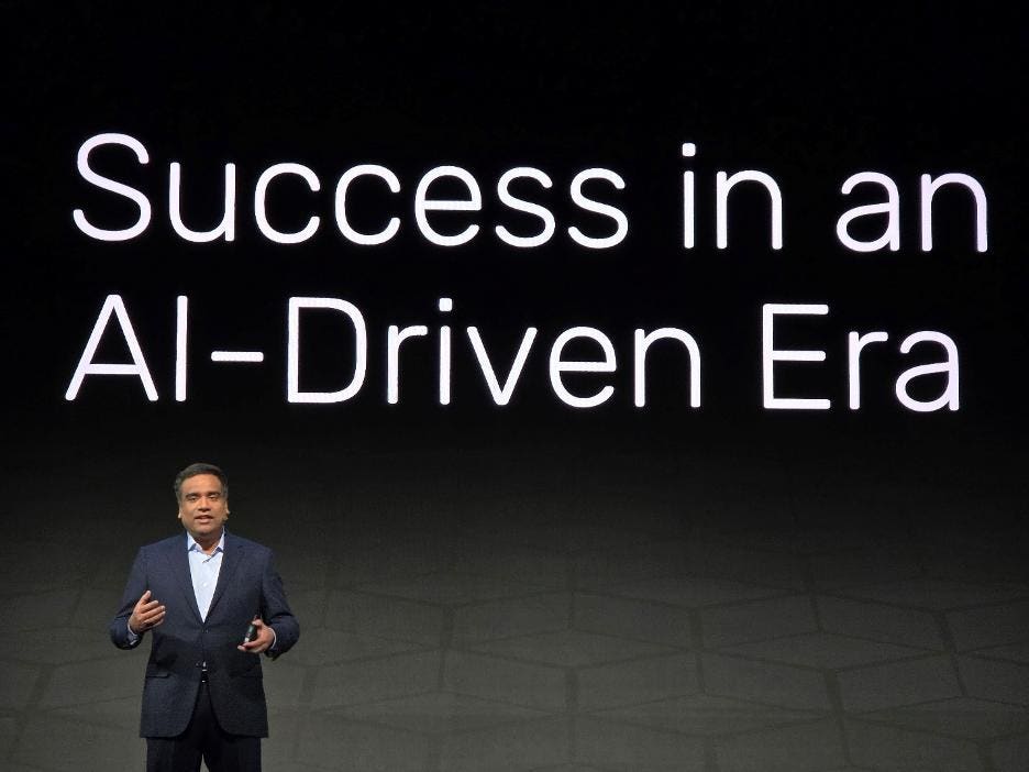
Semiconductor industry is evolving rapidly with the rise of AI-powered applications, pushing companies to adopt new technologies like chiplets, die stacking, and new architectures. Cadence, a leading chip equipment and design software company, highlighted its systems-oriented approach at the recent Cadence LIVE event in Santa Clara, California. The company showcased its vision for the future, emphasizing how its products can address complex challenges within the semiconductor industry, from designing transistors to modeling physics simulations for various applications. Cadence’s Cadence.AI platform aims to provide intelligent design acceleration by combining foundational LLMs with generative AI optimizations across different problem sizes.
Cadence’s Dynamic Duo, consisting of the Palladium Z3 and Protium X3 solutions, is designed to accelerate chip design and validation through hardware and software debugging capabilities. The Palladium Z3 features an in-house emulation processor for verifying chip designs before manufacturing, while the Protium X3 platform utilizes AMD’s VP1902 adaptive SOCs for software debugging. These solutions offer faster design bring-up, increased emulation and debugging scale, and higher performance compared to previous generations. Nvidia’s CEO, Jen-Hsun Huang, praised Cadence’s Palladium platform for its role in enabling Nvidia’s new Blackwell architecture, showcasing the importance of collaboration between companies in the semiconductor industry.
Cadence’s Millennium M1, powered by Nvidia GPUs, is a computational fluid dynamics supercomputer that aids in solving engineering problems in industries like aerospace, automotive manufacturing, and energy production. The supercomputer leverages hardware and software acceleration to deliver increased throughput and reduced power consumption for large eddy simulations. Cadence has integrated AI-enhanced features into its EDA, SDA, environmental, and molecular-science tools, enhancing their productivity and effectiveness for chip designers. Customer proof points from companies like Broadcom, Canon, Microchip, and MediaTek demonstrate the benefits of using Cadence’s AI-driven tools for chip design.
Cadence’s software tools, including Cerebrus for digital semiconductor design, Virtuoso Studio for analog and custom designs, Verisium for digital chip verification, and Allegro X for PCB design, leverage AI to improve workflows and productivity for chip designers. The company highlighted how its customers have seen improvements in die area, power consumption, process migration, verification productivity, and PCB placement turnaround time by utilizing these AI-enhanced tools. With the industry moving towards 3-D IC designs and advancements in automotive intelligence, Cadence’s tools and platforms are well-positioned to address the evolving needs of the semiconductor industry and the growing complexity of computational problems.
As Cadence continues to expand its solutions and offerings, the company is evolving into a systems solutions provider that tackles a wide range of challenges in the semiconductor industry. With the increasing demand for semiconductor tools and system-level approaches, Cadence’s AI-enhanced tools are poised to deliver innovative solutions that address the complexity of today’s interconnected world. By collaborating with industry leaders like Nvidia and Tesla, Cadence is at the forefront of driving innovation and enabling the semiconductor world of the future. The company’s commitment to advancing technology and addressing the evolving needs of the semiconductor industry positions it as a key player in shaping the future of AI-powered applications and semiconductor design.


